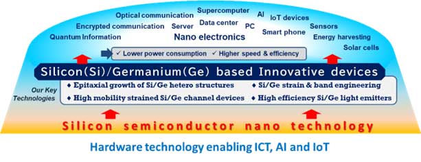
Contributing to our society with Si/Ge-based nano-electronics
Recent expansions of amounts of information and communication have been drastically enhancing power consumptions in computers from data centers to edge devices, imposing world-wide critical problems. We aim to reduce the power consumptions of semiconductor chips by means of introduction of Germanium (Ge) as a novel semiconductor material into the current Si technology. Ge and SiGe have much superior properties to Si, such as high carrier mobilities and light emitting capability. We have wide-ranged technologies of epitaxial crystal growth of Si/Ge hetero structures, strain controlling and band engineering of Si/Ge, with which we are realizing Si/Ge based innovative devices as follows,
High mobility transistors and quantum nano devices using strained Ge channel two dimensional carrier gases
High efficiency light emitting devices and spin LED using strained SiGe/Ge quantum wells
Light emitters and sensors using strained Ge microbridge structures
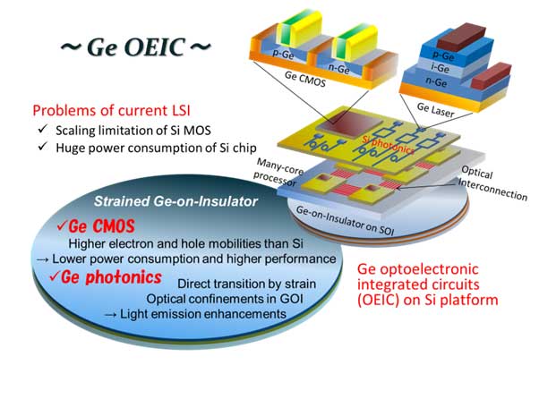
Optoelectronic device integration on Ge platform (GOI wafer)
We fabricate Ge wafer (Ge-no-Insulator, GOI wafer)by Ge epitaxial growth and wafer transfer onto the insulator/Si substrate. On the fabricated GOI wafers, that is, Ge platform we can integrate both electronic and optical devices (Ge Optoelectronic Integrated Circuit, OEIC) consisting of high performance Ge-CMOS and Ge light emitters (lasers), realizing high-performance and low-power-consumption semiconductor chips.