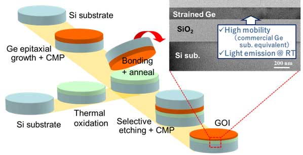
Strained Ge-on-Insulator (GOI) wafer
Toward Ge high performance electronic and optical devices integrated on the same chip, a high quality Ge crystal has to be formed on a Si wafer. We have developed techniques of Ge epitaxy on Si and wafer transfer and obtained high quality strained Ge-on-Insulator (GOI) substrates, having high-mobility carriers in them and capability of light emission at room temperature (RT) owing to the tensile strain induced in the GOI. One of merits of out method is that final thickness of the GOI can be determined by the epitaxial Ge thickness, allowing us to form laterally uniform and very thin GOI, which can be the Ge platform for OEIC.
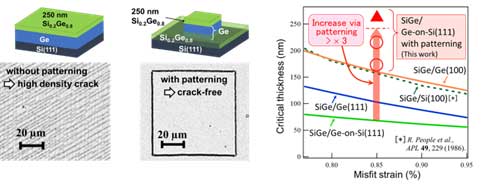
Crystal growth and defects control for strained SiGe/Ge heterostructures
Strained SiGe/Ge hetero structures are attractive for various device applications as they can attain drastic improvements of electrical, optical and spin properties via band engineering. However, due to the accommodated crystal strain exceeding some critical amounts, they inevitably begin to involve crystal defects. We firstly found that high-density cracks are generated in tensile-strained SiGe layers, indicating that it is an issue of critical importance to diminish the cracks for the device applications. We proposed the patterning approach and succeeded in complete suppression of the crack generation in the SiGe layer. Furthermore we study defect generation mechanism in the strained layers and attempt to control dislocation propagation and distribution, leading to defect-free strained layers.
Strained Si/Ge channel 2D carrier gases
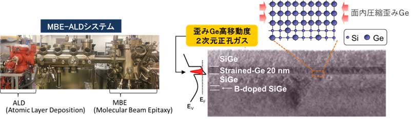
High quality Si/Ge heterostructures are grown with molecular beam epitaxy (MBE), and the highest hole mobility among all semiconductors has been obtained from strained Ge channel which is compressively strained and forms two dimensional hole gas (2DHG) in the Ge quantum well. Various two dimensional carrier gas systems can be created using Si/Ge heterostructures, attracting increased interest toward applications to next generation quantum nano devices. Moreover, by using atomic layer deposition (ALD) system, which is connected to the MBE chamber, we form high quality interfaces between gate insulators and Ge channels, and realize ultrahigh mobility Ge channel MOS devices. Also, ALD can be a powerful tool to passivate Ge surface for Ge-based optical devices.
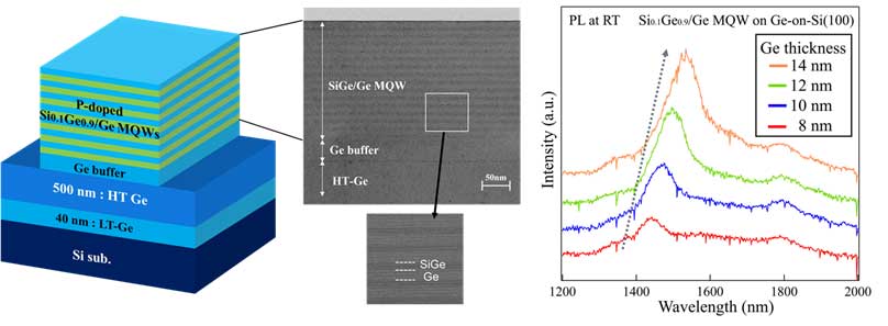
Strained SiGe/Ge quantum hetero structure light-emitting devices
To reduce power consumption in LSI, optical interconnection on the silicon chip has been long anticipated as one of the most promising solutions whereas there has been one critically challenging issue which is the difficulty in creation of high efficiency light sources monolithically integrated on the Si wafer.
To overcome this issue, we study on epitaxial growth of high quality strained Si/Ge heterostructures and SiGe/Ge multiple quantum well structures the Si wafer, and develop high efficiency Si/Ge based light emitting devices enabling on-chip optical interconnection. We have obtained strong room temperature light emission by both electrical and optical pumping owing to carrier confinements in the Ge quantum well.
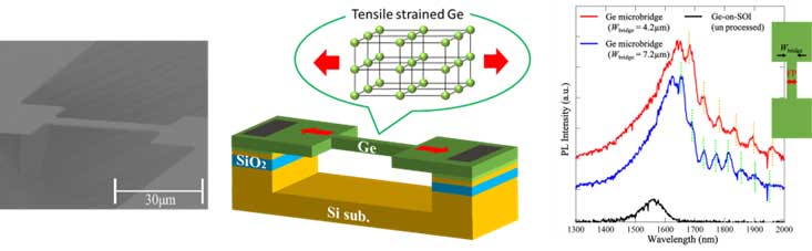
Strained Ge microbridge light emitting devices
Although the Ge is naturally an indirect bandgap semiconductor, its band structure can be highly modified and altered to nearly direct one (Band engineering) by introduction of lattice strain into the Ge crystal, opening new routes to various device applications. We have succeeded in introduction of very large lattice strain into Si/Ge based micro-structures, such as Ge microbridges, which are fabricated with selective etching technique for Ge-on-Si or GOI, and resultantly we obtained strong light emission and resonant peaks owing to light confinements in the bridge. Furthermore, we are developing novel devices with new functionalities by combination with micro resonant structures and MEMS devices.
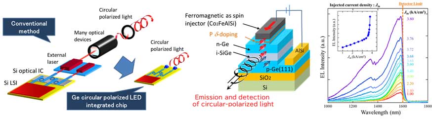
Circularly polarized light emitting Ge spin LED
For encrypted optical communication and medical applications, circularly polarized (CP) light is considered to be utilized. We develop Si/Ge spin LED and laser which can emit the CP light controllably. In general, the CP light is obtained by using large size optical devices, however, Ge spin LED can be integrated on the Si IC chip, which greatly increases feasibility of CP light and widen its applicability to various fields. In the spin LED, spin polarized electrons are injected into the Ge LED through contact electrodes made of ferromagnetic materials, which is epitaxially grown on Si/Ge with high quality interfaces by Prof. Hamaya’s group in Osaka Univ. under the collaboration between Osaka Univ. and TCU. Recently, we have obtained strong room temperature EL emission from fabricated spin LED structures and CP light evaluation is now undergoing.